20.109(S24):M2D7

Introduction
The Transmission Electron Microscope (TEM) achieves its remarkable resolution by 'illuminating' samples using an electron beam in a vacuum rather than using a conventional light source in air. TEM enables 0.14 nm resolution. At this resolution, one can distinguish individual planes of atoms – making TEM an excellent materials characterization instrument. The visualization of single atoms allows one to determine many parameters that describe the structure of the material, such as crystal plane spacing. Additionally, TEMs can be equipped to perform energy-dispersive X-ray spectroscopy analysis (EDX/EDS/XEDS) or electron energy-loss spectroscopy analysis (EELS). The former, EDX, enables identification of the atomic composition of heavier elements in the material. EDX has limited detection of elements below sodium (Na) on the periodic table and no detection of elements below carbon (C). The latter, EELS, is most sensitive to lighter elements, typically from carbon to the 3d transition metals. EELS can reveal atomic composition, electronic properties of the valence and conduction band of a material, surface properties, and chemical bonding.
Although we will be using TEM for materials characterization, it should also be noted that TEM is used for the analysis of biological materials as well. Since the electron beam passes through the sample that is being examined, the sample must be sufficiently thin and sufficiently sturdy to be hit by electrons in a vacuum. Rather than imaging single atoms, biological samples display contrast of components via different densities. Areas of higher density show up as a darker color than areas of low density, creating a "shadow image." It is important to remember that many biological materials are damaged or destroyed by the incoming electrons and that the TEM can image only the species that survive this harsh treatment.
In TEM, the denser parts of the sample will absorb or scatter some of the electron beam, and it's the scattered electrons or those that pass through the sample that are focused using an electromagnetic lens. This "electron shadow" then strikes a fluorescent screen, giving rise to an image that varies in darkness according to the sample's density. For samples that are amenable to TEM, this form of examination can allow observation of ångström-sized objects and of cellular details down to near atomic levels.
The principles behind transmission electron microscopy are analogous to the principles behind an optical microscope. Instead of light and glass lenses, however, the TEM utilizes an electron beam focused via electromagnetic lenses. Since the TEM utilizes an electron beam rather than visible light, the microscope must also function under a vacuum. This condition allows the electrons to remain traveling in a straight line because they have no air particles with which to collide.
Specifically, at the top of the column of a TEM, a high voltage electron beam is emitted by a cathode and focused via a condenser lens. Then the beam is transmitted through the specimen. The resulting image is then magnified through a series of electromagnetic lenses until it is recorded by a fluorescent screen or camera.
Protocols
Part 1: Examining TEM images
- We will be imaging our quantum dots via TEM. To prepare for TEM, your previously collected samples were dotted onto a very thin TEM grid.
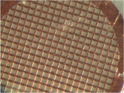 Copper TEM grid with carbon mesh, photographed at 60X magnification
- TEM grids can be made of many kinds of materials. Each design, however, includes lines of a conductive metal which disperses the electron beam and thereby prevents destruction of the sample from the harsh beam.
- Our TEM grids are composed of a copper mesh with carbon mesh is strung between the grids.

To prepare grids to image quantum dots, the following steps were performed in the Belcher lab.
- Sonicate yeast to dislodge quantum dots from cell surface
- Pellet sonicated samples at 1000 x g to remove debris, and transfer supernatent to a clean tube.
- Vortex the supernatent for at least 1 minute and immediately remove 10 μL of the quantum dot suspension to place on the TEM grid that you have balanced in the tension tweezers. Treat the grid with care and use the tweezers only on the edge to minimize damaging the delicate mesh.
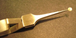 TEM grid balanced in tweezers, wrong side up!
- Allow the quantum dots to settle onto the grid undisturbed for 10 minutes.
- Remove the droplets of water from the grids by touching the edges with a Kimwipe, thereby wicking the solution off the grid.
- Wash the grids by adding 10 μL of sterile water onto each grid.
- Allow the grids to sit with water for 1-3 minutes and then wick dry.
- Wash the grids by adding 10 μL of 100% EtOH onto each grid.
- Allow the grids to sit with EtOH for 1-3 minutes and then wick dry, if it hasn't air dried.

- Once a sample has been applied to our TEM grids, we will only visualize the portions of the sample contacting the carbon mesh, along with any imperfections in the carbon mesh itself.
Today you will image the TEM grids that contain your quantum dots. Due to space limitations, only 2 groups can join Prof. Belcher and Dr. Jifa Qi for the imaging at a time.
Next day: Complete data analysis and organize Research Article figures