Difference between revisions of "Electronics primer"
Steven Nagle (Talk | contribs) (→Diodes) |
Steven Nagle (Talk | contribs) (→Diodes) |
||
| Line 218: | Line 218: | ||
|} | |} | ||
| − | + | ==Diodes== | |
[[Image:Diode_IV_Curve.png|300 px|thumb|right|Diagram of the IV curve for a basic diode with reference to its circuit schematic symbol, showing direction of current flow from terminal a to terminal b.]] | [[Image:Diode_IV_Curve.png|300 px|thumb|right|Diagram of the IV curve for a basic diode with reference to its circuit schematic symbol, showing direction of current flow from terminal a to terminal b.]] | ||
Revision as of 15:29, 9 September 2013
Circuit models
The physical quantities that characterize many types of systems are defined at all points in space and time. For example, Maxwell's equations describe the relationship between the electric field, magnetic field and charge at every point in space and time. The equations govern the operation of electric circuits. Computing the field and charge at every point is a very thorough approach to analyzing an electrical system. However, such a detailed model includes far too much information than is practical or necessary.
Analysis of many systems can be dramatically simplified by using circuit models. Circuit models characterize a system only at a small number of well-defined points by collapsing regions of space into lumped elements. A circuit model is a representation of a system that consists of a network of lumped elements connected together by wires. Regions of space that do not significantly impact system behavior are ignored.
Lumped elements are idealized abstractions of physical components, such as a resistors. Elements are bounded by terminals. Every element obeys a constitutive equation that describes the relationship between the state variables at its terminals. In elements with two terminals, one is typically designated (+) and the other (-). Each type of element has an associated graphic symbol. Symbols can be arranged in schematic diagrams to depict a system of interconnected elements. The symbol for a resistor is shown at right. It is possible to create lumped element models of many types of systems that have two state variables, including thermal, acoustic, hydraulic, and mass-spring-damper systems.
The state variables for an electric circuit are voltage (v) and current (i). Current measures the flow rate of charge carriers moving through the element. Voltage quantifies the electrical potential difference between two terminals. Higher voltages attract charge more intensely and thus result in larger current flows. Every two-terminal element has a single voltage across it and current flow through it.[1] The constitutive equation for an ideal resistor is given by Ohm's law, v=iR.
This page introduces the ideal electronic elements and reviews methods for solving circuits.
Review of electrical units and equations
- Electric charge is measured in Coulombs, usually abbreviated with a capital C. Electrons have a charge of about 1.610×10⁻¹⁹ C. (One mole of electrons has a charge of about 96500 Coulombs.)
- Electric potential difference has the units of energy per charge and is measured in Volts. 1 Volt = 1 Joule/Coulomb = 1 kg m2 / sec 2/Coulomb. The variable v is most often used for voltage.
- Current flow has the units of charge per time and is measured in Amps. 1 Amp = 1 Coulomb / sec. [2] The variable i is normally used for current.
- Resistance has units of Ohms. 1 Ohm = 1 Volt divided by 1 Amp. Resistance is usually denoted by R
- Electric power is equal to voltage times current, P = v i. Power has units of energy per time called Watts. 1 Watt = 1 Volt x 1 Amp = 1 Joule / second.
Networks of lumped elements
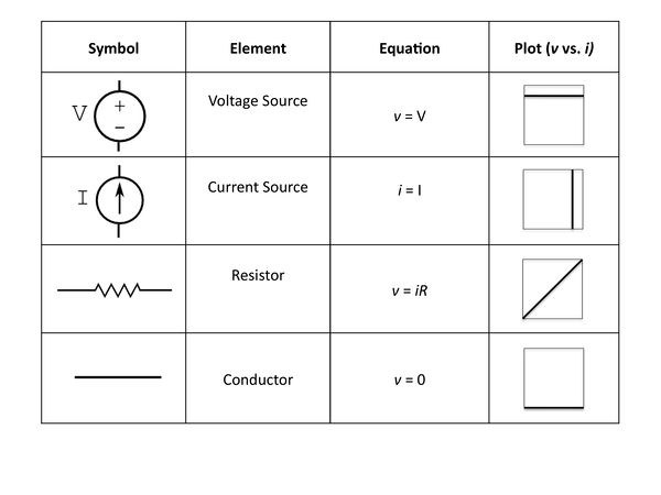
Table 1 lists the name, symbol, constitutive relation and its graphical representation for four ideal elements: a voltage source, a current source, a resistor, and a conductor. Each constitutive equation and associated plot relate voltage (v) across an element and current (i) through that element.
|
| Table 1: Constitutive relations for ideal elements. |
An ideal voltage source maintains a constant potential difference across its terminals regardless of the amount of current flowing through it. Thus, its voltage versus current graph is a horizontal line. The current flowing through an ideal current source is constant no matter what potential difference is across its terminals. The ideal resistor obeys Ohm’s law, $ v = iR $ — a sloped line on the voltage versus current graph. Ideal conductors have zero resistance, meaning that the voltage at all points on the conductor is the same for any value of current flow.
To form a network of elements, terminals are connected together by ideal wires. Elements interact only through their terminals. Terminals may be shown as filled or open circles to indicate whether or not that terminal connects to another electrical element. (Open circles represent no connection.) Pairs of terminals are sometimes called ports, whether for a single element or across multiple elements. A port approach is particularly useful for abstracting away (black-boxing) multiple circuit elements and treating them as an equivalent element with defined inputs and/or outputs. We'll return to this idea in sections 5.4 and 5.6.
A voltage v and current i can be defined at any terminal. For terminals A and B in Figure 1, the element voltage $ v = v_{AB} = v_A - v_B $ and the element current $ i = i_A = i_B $. Here, $ v_A $ and $ v_B $ are the absolute potentials (defined relative to a reference), and v is the potential difference between the two terminals.
Two limiting cases of the resistor element are useful for solving circuit problems: the open circuit and the short circuit (Fig. 2). Infinite resistance means that no current passes through that element; this is also called an open circuit across said element and is equivalent to an unconnected port. Zero resistance means no potential difference appears across the element; this is also called a short circuit across that element and is equivalent to an ideal wire.
Connecting circuit elements
Multiple elements may be joined at their terminals to build a circuit (Fig. 4). The joined terminals are now called nodes. Any path between two (independent -- see below) nodes is called a branch. Any path from one node back around to itself is called a loop. We’ll revisit these terms when we solve circuit problems in section 5.
Note that two (or more) apparent nodes that are connected by an ideal conductor are considered equivalent, because the conductor by definition cannot maintain a potential difference. Thus, A and the (A)'s above represent only one independent node, not three, as do B and the (B)'s. The two Steve's are of course independent nodes :)
Now is a good time to emphasize the difference between an element variable and a node variable. The element voltage $ v_{AB} $ is defined as $ v_{A} - v_{B} $. In other words, an element voltage equals the potential difference across the terminals, while a node voltage equals the absolute potential at a terminal. Of course, this "absolute" potential must still be with respect to a common reference point.
Series and parallel
When two elements are joined end to end, they are said to be in series. In this case, the (-) terminal of one element is joined to the (+) terminal of the second element. If instead the (+) terminals of the two elements are connected, as are their (-) terminals, then the elements are said to be in parallel.
Resistors in series are additive: $ R = R_1 + R_2 $.
Resistors in parallel are inversely additive: $ \frac{1}{R} = \frac{1}{R_1} + \frac{1}{R_2} $, and thus $ R = \frac{R_1 R_2}{R_1 + R_2}. $
The current that flows through each resistor in series must be identical, while for resistors in parallel, the voltage across each one must be identical. We will learn why when we discuss Kirchoff’s laws in section 5.1.
Similarly, voltage sources connected in series are additive, with current unaffected. Voltage sources linked in parallel maintain the potential difference of a single voltage source (so all sources must be identical or things get tricky ), with increased current flow.[3]
Series and parallel relationships can be used to reduce complex circuits to more simple ones as an intermediate step in problem-solving.
Ground
Note that a voltage, or potential difference, is always a relative description. For example, for a voltage source the nominal (supposed) voltage -- say, 12 V -- is the potential difference between the (+) and (-) terminals. It is usually really convenient when solving circuit problems to define the (-) terminal as zero. (The relative nature of voltage allows this arbitrary choice.) This potential level is called ground. Ground can be considered a reservoir of electrons. By definition, any terminal connected to ground by a wire must also be at 0V. Ground is also the usual reference point for defining terminal/node voltages.
However, there is nothing stopping us from defining the (+) and (-) terminals as +6V and -6V, and this may be convenient in certain problems.
Understanding equivalent diagram topologies and notations, part 1
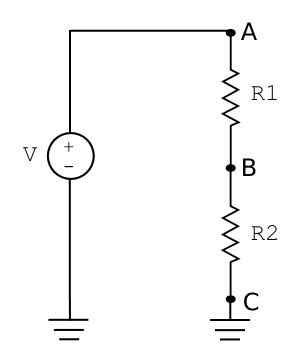
A common group of elements comprises a voltage source and two resistors in series. For reasons we shall see shortly, this grouping or "primitive" is called a voltage divider. Two common ways to depict this circuit are shown below.
We can see that the voltage at node C is trivially 0, and that at node A is the maximum source voltage, because these are connected to the voltage source by ideal wires. The voltage at node B depends on the relative values of the two resistors.
As an example, let's take V = 12 V, $ R_1 $ = 200 Ω, and $ R_2 $ = 600 Ω. Each resistor is described by $ v=iR $, where i must be uniform in this purely series-connected circuit. Ohm's law also applies to the circuit as a whole when using the overall series equivalent resistance $ R_{eq} $, namely the sum of the two resistances. Thus, $ v = 12 \text{V} = i R_{eq} = i (R_1 + R_2) = i (200 + 600)\Omega $, which can be solved for i = 15 mA.
The first resistor is described by $ v_{AB}= i R_1 =15 mA * 200 \Omega $. Thus, it has an element voltage of $ v_{AB} = 3 \text{V} $, and the node joining the two resistors has node voltage $ v_B = 12 - 3 = 9 \text{V} $. Indeed, solving the second resistor equation $ v_{BC}= i R_2 =15 \text{mA} * 600 \Omega $ yields 9 V (with $ v_C $= 0 , of course).
Clearly, a voltage divider "divides" the voltage drop across resistors in series in proportion to their resistances. In sections 5.2-5.3 we will see a more universally applicable way to solve this problem, when we cannot rely on our intuition as much. Then we will imagine connecting measurement devices to the circuit and also further discuss topology.
Some other examples of topogically equivalent circuits are shown below (Fig 8).
Putting it all together: solving circuit problems
Solving problems: fundamentals/theory
Two key relationships provide the foundation for circuit analysis: Kirchoff’s circuit law and Kirchoff’s voltage law, hereafter KCL and KVL. KCL is based on charge conservation: at any node, the sum of the current magnitudes flowing in must equal the sum of the current magnitudes flowing out. When solving problems in which current directions are trivially known, this form of the law works well.
And now we see why current must be equal for elements connected in series: at the shared node, current coming out from the first element must have the same magnitude as current coming into the second element. No other branches exist at that node.
Returning to the issue of signs, current always flows from the (+) to the (-) terminal for an element, that is, from higher to lower voltage (except in a voltage source). However, the terminal definitions may not always be obvious/known in advance of solving the circuit problem. To keep signs straight, it will be convenient to have a systematic relationship between i and v signs. This relationship is described in the problem-solving section just below.
KVL is based on conservation of energy: the sum of the element voltages (potential difference across each element) around a loop is zero. Equivalently, the potential difference between the starting and ending node in a loop (that is, the same node) must be zero.
Take, for example, the three node voltage divider from section 4.3. Applying KVL directly in a clockwise direction, $ v_{AB} + v_{BC} +v_{CA} = 3+ 9 -12 =0. $ KVL is even more straightforwardly applied using node voltages. Again going clockwise, clearly node voltages $ v_A - v_B + v_B - v_C - v_A + v_C = 0 $, without even plugging in numbers.
Now we also see why voltage must be equal for elements connected in parallel: the two shared nodes form a loop, and hence the potential differences across the two elements must be identical.
Solving problems: node-voltage analysis method
One rigorous way to solve circuit problems is to write the constitutive relation for each element (B equations for B branches), every independent KCL statement (N-1 equations for N nodes), and every independent KVL statement (B-1+N equations for B branches). Then algbraic substitutions are made until every element voltage and current is known. Often it is not obvious which substitutions will most quickly yield the quantities that are actually of interest in that problem.
The node-voltage analysis method is a faster universal approach for solving circuit problems. It indirectly incorporates KVL and requires fewer KCL statements. Rarely can there be confusion about which choice of equations will quickly yield meaningful results. (For very complex circuits, however, linear rather than simple algebraic approaches may be required.)
Recall that while an element voltage is the potential difference across said element, a node voltage is the potential difference between that node and a common reference point – usually ground. (If these definitions don't sound familiar, see Figure 1 under Primary definitions and also review Connecting circuit elements.)
Working with node voltages rather than element voltages makes KVL implicit, as we saw in the voltage divider example above. The basic approach is then to write a single KCL equation per unknown node voltage, while immediately substituting in the element constitutive laws in terms of voltages and resistances.[4]
Now we make our alternative statement of KCL: the sum of all currents flowing into a node is zero, where current now includes both magnitude and sign. By definition, voltage is defined to decrease in the direction of positive current flow. Furthermore, by convention current is usually drawn into the node. Life will be far easier if you adhere to this convention. If the sign of any current turns out to be negative, then that current is actually flowing out of the node.
Understanding equivalent diagram topologies and notations, part 2
Let’s return to the two-resistor voltage divider described in section 4.3 above to practice our systematic approach for solving circuits, calling the single non-trivial node of interest B for consistency. We can apply KCL to calculate it:
$ i_1 + i_2 = 0 = \frac{12-v_B}{200} + \frac{0-v_B}{600} \to \text{nominal}\ v_B = 9 \text{V}. $
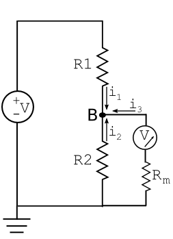
Now let’s imagine connecting a voltmeter to measure the voltage at node B. To read the correct relative potential, the voltmeter must also be connected at ground. In other words, the second resistor and the voltmeter with associated resistance $ R_m $ are in parallel. Before attaching the voltmeter, the access port of interest can be shown as:
After attaching the voltmeter, three equivalent circuit diagrams depicting the system are:
The voltmeter must have a high enough resistance that it does not draw current and substantially affect $ v_B $. If instead it has a comparable resistance, say 300 Ω, let’s calculate the effect on $ v_B $ using our usual KCL approach:
$ i_1 + i_2 + i_3 = 0 = \frac{12-v_B}{200} + \frac{0-v_B}{600} +\frac{0-v_B}{300} \to \text{nominal}\ v_B = 6 V. $
This value is unacceptably far off from our nominal 9 V. However, if $ R_m $ is increased an order of magnitude, to 3 kΩ, $ v_B $is a respectable 8.57 V. (Try it!)
Wouldn't it be nice to calculate $ v_B $ for a given $ R_m $ without repeating the full calculation each time? The next section describes just such a method.
Thevenin equivalent circuits
Topological equivalence between circuits implies that wires have been moved around or added in place of shorthand. There is also such a thing as functional equivalence between circuits. In fact, any complex circuit consisting only of voltage sources and resistors can be reduced to a circuit with only a single voltage source and resistor! This equivalent circuit cannot be empirically distinguished from the multi-component one.
Let’s return to the voltage divider example with a port across the second resistor. We want to know how the circuit as a whole responds at this access port when there is no load on it, i.e., no element in which energy can be dissipated. We calculate the equivalent circuit by three steps.
First we calculate the open circuit voltage ($ V_{oc} $) at that port, namely 9 V as above in section 5.3.
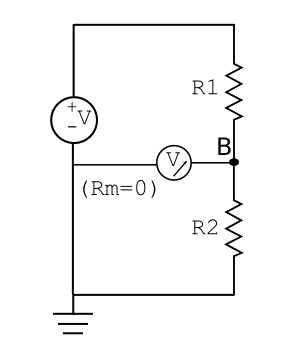
Next we calculate the short circuit current. In this hypothetical, the attached voltmeter has no internal resistance and behaves as a wire (Fig 12). In turn, $ v_B $ is shorted to ground, and current magnitude is dependent only on $ R_1 $, not both $ R_1 $ and $ R_2 $. Hence, the short circuit current $ I_{sc} = 12 \text{V}/200 \Omega = 0.06 \text{A} = 60 \text{mA} $.
Finally, the Thevenin resistance $ R_{Th} = \frac{V_{oc}}{I_{sc}} = \frac{9 \text{V}}{0.06 \text{A}} = 150 \Omega $. The Thevenin equivalent circuit is shown in Figure 13.
Now how does this two-component circuit reduction help us? The voltmeter (or any element!) can be connected in series with $ R_{Th} $, and $ v_B $ calculated immediately by the simple voltage divider relation, $ \frac{V R_m}{R_{tot}}. $
An alternative and direct calculation of $ R_{Th} $ is the total resistance at the port as viewed looking into the circuit (with voltage sources changed to wires): here, $ R_1 $ and $ R_2 $ in parallel.
Alternative problem-solving strategies
Circuit problems can be approached in many ways[5] and in the interests of time we will primarily treat the approach that (nearly) universally works, namely the node-voltage analysis method described above. Let’s briefly look at one example of another approach that can be used on it's own or can simplify a complex topology before employing the node-voltage method.
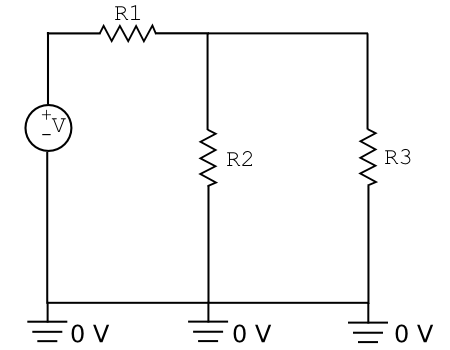
Consider the circuit shown at right. The parallel resistors $ R_2 $ and $ R_3 $ can be temporarily collapsed into an equivalent single resistor. Its resistance is given by
$ R_{parallel} = \frac{R_2 R_3}{R_2 + R_3} = 200 \Omega. $
Then, the current through the purely series-connected circuit is simply
$ i = \frac{V}{R_{tot}} = \frac{V}{R_1 + R_{parallel}} $
where $ R_{tot} = 400 \Omega $ and by the voltage divider relation $ v_A $ is clearly 6 V. That is, half the voltage drop occurs across each 200 Ω resistor, the physically real one and the imaginary one (equivalent to two real ones).
We next expand the circuit to once more include the real, parallel branches. The potential difference across each branch must be the same $ v_A $, and thus the individual currents can be calculated from $ v_A =i_{branch x}R_{branch x} $.
For example, $ i_2 =\frac{v_A}{R_2} = \frac{6}{300} = 20 \text{mA} $.
As expected, $ i_2 $ and $ i_3 $ sum to the current through the first resistor.
Yet another general circuit-solving approach is applying energy conservation equations.
Capacitors
RC circuits
Diodes
Diodes, photodiodes and light-emitting diodes (LEDs) are non-linear devices that function as electronic check valves. The photodiode and LED have additional properties discussed below, while a basic diode is utilized purely for its unique IV curve. An ideal diode allows any amount of current to flow in only one direction, with zero voltage drop, while allowing zero current in the other direction, regardless of the voltage drop. The direction of allowed current flow is called the forward direction and is defined as extending from terminal a (+) to terminal b (−). On a schematic it is denoted by the direction of the triangle in the symbol. It is also shown by an arrow in the IV curve illustration.
In a real diode, high current will lead to damage or destruction. A forward bias, or small voltage drop, must be applied from terminal a to terminal b to cause forward current to flow. This is called the threshold voltage Vth or thermal voltage and depends on the temperature and the quality of the diode. In the transition between 0 V and Vth the current is an exponentially increasing function of the forward bias voltage VD. For the silicon photodiode in this lab, the threshold voltage is approximately 0.7 V.
Photodiodes have all the qualities of a basic diode but are fabricated to enhance their response to light. When light shines on a semiconductor, the photoelectric effect leads to the generation of additional charge carriers. In a diode, which is created by joining an n-type semiconductor and a p-type semiconductor, there is a small region at the junction where the free carriers of the semiconductor are depleted. Across this so-called depletion region there is an electric field.[6] When the applied light creates additional charge carriers, say, electrons, they are swept across the depletion region in the direction of greater potential. In the case of the photodiode in this lab this is toward terminal a, according to the previous paragraph. Recall that the arrow showing positive current almost always represents negatively charged electrons flowing in the opposite direction. In the photodiode it so happens that there are also positively charged free carriers traversing the device in the direction of the arrow. There is one positive charge carrier, a hole, generated for every electron that results from the energy of an incident photon. Thus the net current flowing through the photodiode is made up of electrons flowing toward terminal a and holes flowing toward terminal b. The current flow due to light flux occurs either when the diode is forward or reverse biased. Run in reverse bias, the current out of the photodiode is linearly proportional to the light power striking the device.
Light-emitting diodes (LEDs) are designed to output light when current passes through them. In this case, we have recombination of electron-hole pairs producing photons in the semiconductor. Light is emitted in forward bias, and power output depends on the current through the device.
All diodes exhibit breakdown when a large reverse voltage (typically > 50V) is applied, typically destroying the diode. Zener diodes however are designed to have a relatively low but precise breakdown voltage. These diodes are operated in reverse bias and are typically used as voltage references or to limit the voltage at a one particular node.
Hydraulic circuits
The concepts of electron flow and voltage are far removed from everyday experience; however, most everybody has used a water spigot, garden hose, and bucket. For this reason, many people find hydraulic circuits more intuitive than electronic circuits. The equations that govern simple hydraulic and electronic systems have exactly the same form, with the state variables of voltage and current replaced by pressure and flow rate. Hydraulic circuits can be a useful metaphor for electronic circuits.
In an electric circuit, increasing the voltage across a resistor increases current, per Ohm's law. The analogous relationship holds for hydraulic circuits: increasing the pressure across a hydraulic resistor increases fluid flow through it. The constitutive relation for a hydraulic resistor is P=QR, where P is pressure, Q is flow rate, and R is hydraulic resistance. A large pipe has a low fluidic resistance, while a narrow constriction has a high resistance. (New figure)
Pressure sources are analogous to voltage sources. Most spigots supplied by a municipal water utility approximate a pressure source. The pressure does not vary much regardless of how much water is drawn from the spigot. (This may not be the case if you live an a house or neighborhood with very old plumbing.)
Hydraulic RC circuit
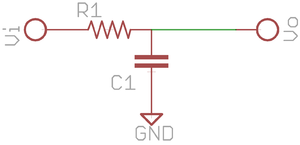
The hydraulic analogy is helpful in visualizing the transient time behavior of an RC filter. The capacitor is a storage device that can be modeled as a bucket containing fluid. The capacitor bucket can be filled as fast as a supply reservoir can deliver the fluid through a hose connecting their bases. The supply reservoir in this analogy has a width Ws >> Wc, that of the capacitor bucket, for the same depth into the page. Flow from supply reservoir to capacitor bucket is proportional to the difference in fluid levels and the fluid level in the supply reservoir is unchanged during the experiment.
The difference in height is called a hydraulic head and represents stored gravitational potential energy. When the level in the supply reservoir is higher, fluid will flow into the capacitor bucket as soon as a valve is opened. The opposite is also true. If someone were to step on the hose, the restriction would result in a slower flow rate. If the capacitor bucket width and the hose restriction are great, the bucket will require a long time to fill. If either the bucket were smaller or the restriction were less, then less time would be required. As the fluid level in the capacitor bucket approaches that of the supply reservoir, the flow between them also slows. Thus if the mass of the fluid is ignored then an exponential decay of flow rate is observed and is a function only of the restriction in the hose, the capacity of the bucket and the initial difference in fluid levels.
The RC circuit is analogous to this simple bucket model
- Electrical charge is analogous to fluid volume. A power supply is a charge supply reservoir. A capacitor stores charge on two opposing plates in an electric field, a situation that is analogous to the difference in fluid levels in a gravitational field.
- The size of the resistor R1 is analogous to the amount of restriction in the hose.
- Current flow through the electrical resistor is analogous to fluid flow through this restriction.
- The magnitude of the capacitance C1 is analogous to the width Wc of the capacitor bucket, all else being held constant.
- The difference between the capacitor voltage Vo and the supply voltage Vi, which is also the voltage across the resistor R1, is analogous to the difference between the fluid levels in the bucket and the reservoir.
In this model, the RC time constant τ = R1C1 of the electrical circuit is proportional to the time required for the capacitor bucket fluid level to rise to (or fall to) that of the supply reservoir. In the electrical circuit, it is the time required for the voltage Vo to change by 63% of the initial difference between voltages Vi and Vo. It is also commonly referred to as the relaxation time.
Other circuit analogies
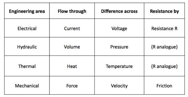
Several analogies to electronic circuits can be useful to the novice in understanding the laws that govern the state variables current and voltage. In particular, the basic hydraulic analogy often provides an intuitive model when first learning circuit behavior. In general, circuit models are useful for solving a wide variety of problems in other engineering domains — electrical, mechanical, thermal, acoustic and several others including hydraulics. Anything that is well described by a system of linear ordinary differential equations is amenable to circuit analysis.
References
- ↑ For more about circuit assumptions and abstraction layers, see Agarwal 1.1-1.4: The power of abstraction, The lumped circuit abstraction, The lumped matter discipline, and Limitations of the lumped circuit abstraction.
- ↑ By convention, current is positive in the direction of positive charge flow, which means the electrons are actually flowing in the negative direction.
- ↑ See Agarwal 1.5.1, Practical two-terminal elements: Batteries, for more information.
- ↑ Slightly more complex approaches must be taken for cases in which a voltage source has a negative terminal that is not connected to ground. See Agarwal 3.3.2, The node method: Floating independent voltage sources.
- ↑ Overall, see chapters 2 (Resistive Networks) and 3 (Network Theorems) of Agarwal. Section 2.4 (Intuitive method of circuit analysis: series and parallel simplification) treats series/parallel reductions, section 3.5 (Superposition) treats superposition, etc.
- ↑ The field is actually due to the depletion, which itself is caused by thermal motion of oppositely charged free carriers in the two semiconductors, but this is not important here.


