Electronics Mini-Lab
Overview
During the next lab exercise on measuring DNA melting curves, you will build and debug several electronic circuits. This mini-lab will introduce you to the electronic components and test equipment you will use. A short answer-book style writeup is required. Items to include in your report are shown below in bold.
This mini-lab requires an understanding of basic circuits. If you need to review circuit concepts, start with the Electronics Primer page. If you have a lot of experience with electronics, ask one of the instructors about doing a stimulation mini-project instead of the mini-lab assignment.
Making and characterizing a resistive voltage divider circuit
In the first part of the mini-lab, you will analyze and build a voltage divider. The divider circuit comprises two resistors and a voltage source, as shown in the schematic diagram. You will select the values for R1 and R2. Choose any resistor values you like, but there are a few practical constraints.
The resistors in the lab range in value from 1 Ω to 10 MΩ. Within that range, manufacturers only produce certain standard values. Check the supply bins or this table to see which values are available.
Power dissipation in resistors increases in proportion to the resistance and as the square of current, P = I 2R. The maximum power rating of the resistors in the lab is 1/4 Watt. Components operated at too high a power level may get very hot and fail. A noxious puff of smoke frequently accompanies failure. Even if a component operated at an excessive power level does not completely fail, it may no longer behave as specified. Ensure that the power dissipated by R1 and R2 does not exceed the maximum rating.
You will use an oscilloscope and a volt meter to measure voltages in the circuit. The oscilloscope has an input impedance of 1 MΩ. Connecting the oscilloscope probe to a node of the circuit is equivalent to placing a 1 MΩ resistor between that node and ground. In circuits that use very large resistors, the current flowing into the oscilloscope can significantly distort measurements.
Before building the divider circuit:
- Record the resistor values you selected and the gain of the circuit, Vout / Vin.
- Derive the voltage Vout for the voltage divider circuit.
- Plot an IV curve consisting of calculated current I on the vertical axis versus Vin on the horizontal axis over the range 0 V < Vin < 15 V.
- Derive a formula for the power dissipated in R1 and R2 as a function of Vin.
- Add the power dissipation to the plot of the IV curve.
- Derive a formula for the change in Vout if a 1MΩ resistor is added in parallel to R2. Show the equivalent circuit and your derivation.
Measuring resistance with a digital multimeter
Go ahead and get the resistors for your circuit from the bins in the lab.
According to the manufacturer, the actual resistance of the resistors we use in the lab may differ from their nominal value by up to 5%. You can get more accurate results by measuring the actual value of the resistors you use with a digital multimeter (DMM). DMMs are multifunction instruments that usually include functions for measuring voltage, current, and resistance.
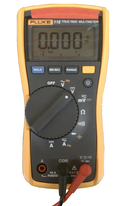
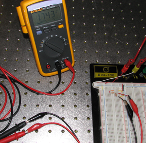
Plug a set of test leads into the DMM. The black goes into the terminal labeled COM. The red lead plugs into different terminals depending on the measurement you are making. To measure resistance, plug the red lead into V/Ω. The A terminal is for current measurements.
- If you have read ahead and already connected power to your circuit, make sure it is off.
- Disconnect the resistor you want to measure so that other parts of the circuit will not affect the resistance you measure.
- Switch the DMM to resistance mode, which is labeled with the Ω symbol.
- Place the DMM leads in parallel with the resistor of interest.
- Read and record the value on the DMM. Repeat for the second resistor.
- Calculate and record the difference from the specified value.
The manufacturer's tolerance for the resistors in the lab is 5% of the nominal value. Therefore, the resistances in the circuit you build will be somewhat different than the nominal values you analyzed.
Solderless electronic breadboards
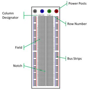
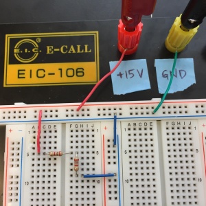
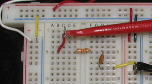
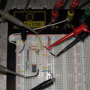
Most electronic components look like bugs. They have a central body with a bunch of gangly legs sticking out, called leads. The leads carry current from the outside of a component to its innards. One of the first challenges facing an aspiring circuit maker is to properly connect all the bugs' legs whilst keeping the circuit robust and orderly. Solderless electronic breadboards are a convenient platform for building circuits that might require a lot of debugging or frequent reconfiguration. Breadboards have a large number of square holes in them called tie points. A single wire or component lead fits into each tie point. Spring-loaded contacts inside each tie point hold leads in place and provide an electrical connection. The images below show examples of solderless electronic breadboards.
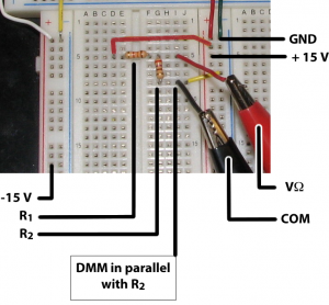
Sets of tie points are electrically connected in a pattern that allows component leads to be connected in almost any arrangement. The two central grids of tie points separated by a notch are called the field. Each row of tie points in the field is called a terminal strip. The terminal strips are numbered. Columns are designated by a letter. Within a terminal strip, the five tie points A-E are connected, and tie points F-J are connected. Points A-E are not connected to points F-J. Connections between component leads are made by running jump wires between tie points that are connected to each lead, as shown in the image above on the right.
The lines of tie points to the left, right, and above the field are called bus strips. Bus strips are highlighted by red and blue lines. All of the tie points in a bus strip are connected together. Because most circuits have a lot of power and ground connections, the bus strips are almost always connected to the power supply. Using the bus strips as a power distribution network makes it easy to connect any terminal strip to power or ground with a short jump wire.
If you are unsure whether two holes on the breadboard are connected, insert short wires in the holes. Use the resistance or continuity features of the DMM to check if they are connected.
There are a few downsides to breadboards. They have high interconnect capacitance and resistance. If you don't know why that's bad, pay attention in lecture over the next few weeks.
Build the circuit
- Gather components to build the divider circuit:
- solderless electronic breadboard
- lab station with a working power supply and digital multimeter (DMM)
- jump wires, or a few lengths of different colored wire (located near the breadboards)
- wire strippers (located in your lab station drawer)
- banana cables (located on the West wall)
- resistors of the selected values (located on the bench at the North wall)
- Verify the value of the resistors by reading the coded bands.
- Through negligence or malice of last semester's scholars, components occasionally end up in the wrong bin. Instructions for reading resistor markings are available at this website.
- Mount the resistors by pressing component leads into the tie points in the field.
- Trim the resistors leads to keep the component body close to the board. This will also prevent long leads from shorting on the bottom metal of the board.
- Run jump wires to connect the divider to power and ground bus strips.
- Keep your wiring neat, close to the board, and easy to follow. A good way to do this is to route wires horizontally or vertically, making right-angle bends to change directions.
- Use the right length of wire. The right length of wire is the shortest length of wire that satisfies the previous guideline.
- Use the bus strips to distribute power supplies and ground.
Connect the power supply
The lab power supplies provide three voltage outputs. The (+) and (−) outputs have adjustable current limits and voltages up to ±20 V can be set either independently, or together (using the mode buttons located between the pairs of voltage and current knobs). While the POWER button at lower left applies power to the supply itself, the white OUTPUT button on the upper left enables power to flow to the outputs: always remember to turn this off or disconnect it when rewiring your circuits. There is also one fixed 5V output at the lower left. Use this output with care, as its current has a very high limit, noted below the terminals as 3 A.
Connecting a wire directly from the power supply to a tie point is tenuous, so the breadboard also has four colored posts, which are visible in the image above right. These are called banana terminals. Each post accepts a banana connector inserted at the top and a bare wire at the base. The wire should be passed through the hole at the base of the post and secured with the colored plastic nut. A cable with banana connectors on both ends connects the power supply to the posts. The banana terminals are not connected to any tie points, so it is necessary to run a wires from the posts to tie points on the bus strips. Then wires must be run from the bus strips to the component power and ground leads.
Note that the green GND connector is connected to the power supply chassis ground (or AC power ground); it is not ground for your circuit.
- Connect the power supply to the breadboard with banana cables.
- Use the black banana connector and blue bus strips for ground. Red bus strips are almost always used for power supplies.
- The exposed metal screws on the bottom of the banana connectors can short to the metal optical table. Cover them with electrical tape to prevent a calamity.
- When making wire connections to the banana terminals, be sure that only bare wire touches the terminal. Insulation under the screw terminal may cause an intermittent connection.
- Connect the power and ground bus strips to the circuit.
Measure voltages with the DMM
The DMM has modes for measuring DC and AC signals. In DC mode, the meter reads the average value of the test signal. In AC mode, the meter reads the root-mean-square value of a time varying signal. In this lab you will use DC mode, which is labeled with a solid line above a dashed line.
- Switch the DMM to DC voltage mode and connect the DMM test leads properly: Insert black in COM and red in VΩ.
- Make firm contact with the two leads across the terminals of R2.
- Record the votlage shown on the DMM for each input voltage Vin = 0, 2.5, 5, 10 and 15 V.
- Include the uncertainty of the measurement.
- Calculate and record the change in the measured voltage if the DMM input impedance were reduced to 1 kΩ.
Measure current with the DMM
- Switch the DMM to DC current mode and connect the leads as shown in the figure above: Positive current is measured into the red lead, moved to the A socket of the DMM, and out of the black lead, remaining in the COM socket.
- Place the leads of the DMM in series with the circuit loop.
- Record the current through the circuit at each input voltage in units of mA.
- For the highest voltage, calculate the effect on measured current if the input impedance were increased to 1 kΩ.
- Using the measured current, calculate the resistance of R2 using Ohm's law and each of the currents and voltages that you measured.
- Calculate the percent error in the measured resistance values.
- Compare to the tolerance value specified by the manufacturer and to the resistance values measured earlier.
- On the same axes as your last figure, plot an IV curve consisting of measured current I on the vertical axis versus measured Vi on the horizontal axis.
Making and characterizing a low-pass RC filter
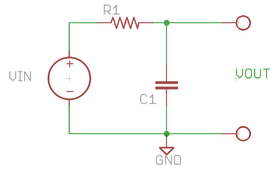
Most signals contain components that are changing with time. The RC filter above is one of the simplest circuits to begin to understand such time transient signals. When R2 is replaced with a capacitor and a fixed Vin is applied, the output voltage Vout is not initially constant as it is for the divider circuit. Instead the voltage Vout approaches Vin over time, quickly at first and then more slowly at an exponentially decaying rate. For this reason the circuit will filter out quickly changing inputs because the output does not respond quickly. It so happens that if we reverse the placement of the resistor and capacitor then this behavior is reversed, but we will come back to that later. For now you will build and measure the low-pass filter shown above.
To make this circuit:
- Turn off the power supply.
- A different type of supply will be connected to the RC filter (see below).
- Remove the jump wire between the voltage divider and the +15 V bus strip.
- Replace R2 with a capacitor in the range of 0.1 - 10 nF, depending on the size of the resistor R1.
- The suggested capacitance range assumes R1 in the range of 100 - 10,000 Ω.
- Don't worry about the precise capacitor value at this time.
To investigate the behavior of the RC filter circuit, a function generator will replace the DC power supply to apply a voltage Vin that varies with time. And the voltage output Vout will be measured with an oscilloscope instead of the DMM above.
Function generator
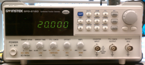
A function generator generates signal waveforms for standard functions: sinusoids, triangles, square waves. The digital function generators in the lab generate waveforms at precise frequencies in the range from 0.01 Hz to 10 MHz, and amplitudes ranging from ±0.1 V to ±10.0 V. Frequencies are entered directly on the number keypad followed by units of Hz, kHz or MHz. The knob on the upper right of the unit can fine tune the frequency.
- Do not yet turn on the function generator.
- Connect the function generator to your circuit:
- Connect the function generator using a BNC cable at the Output connector on the front right of the function generator.
- At the circuit end of the BNC cable, use a BNC adapter ending in either red and black clips or two 21 gauge wire leads.
- Connect the positive lead (the center conductor of the BNC) to the Vin side of R1 and connect the negative lead (the outer shield conductor of the BNC) to the ground bus strip of the breadboard.
Oscilloscope
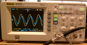
An oscilloscope ("scope" for short) is designed for observing signals that change with time. There is a triggering mechanism by which the oscilloscope determines when to start measuring the signal. The screen of the oscilloscope displays the signal level in Volts versus time in seconds, with the trigger point near the left side of the display. The vertical scale knobs are used to set the voltage fraction per major vertical division on the display. The horizontal scale knobs are used to set the fraction of a second per major horizontal division. The trigger can be set to watch for a rising signal or a falling signal, among others, through the menu button at far right. The signal level at which the trigger is activated can be adjusted with the smaller Level knob, also at the right of the front of the scope. The 309 scopes can also perform many basic measurement tasks such as amplitude, peak-to-peak, frequency, and phase measurements. Most functions are controlled via menus. Basic functions are described below, but full manuals can be downloaded for the Rigol DS1052e and the ATTEN ADS1022c.
- Connect the scope to the circuit.
- Bring two scope probes to your station. They are found on the North wall to the far right of the white board. They are attached to thin coaxial cables with BNC connectors on the end.
- Connect the BNC connector of one probe to CH1 and connect the probe itself to Vout using a small jump wire and the retractable clip at the end. Also connect the black alligator clip to the Ground bus strip.
- In a similar fashion connect the other probe to CH2 and Vin.
- Set the oscilloscope vertical scale for each channel to 5 V per division. Note that the Rigol scopes have one knob for both channels, so first press the button for the desired channel, e.g. the CH2 button assigns the knob to CH2. If you have an ATTEN scope, there is a knob for each channel. However, software menu functions still require you to press the button for the desired channel.
- Set the scope to trigger from CH2, the input channel in this setup.
Measure the low-pass RC filter
- Turn on the function generator and set parameters.
- Enter a frequency of 1 kHz using the number pad and range buttons.
- Press the WAVE button to select a square wave output.
- Adjust the AMPL knob to a desired level by referring to the signal measurement on scope CH2, which is Vin.
- Adjust the horizontal scale of the scope until individual signal periods can be seen clearly.
- Play around a little with the amplitude of the function generator output level and the oscilloscope settings.
- Investigate the behavior of the circuit.
- Try different combinations of resistor and capacitor.
- Adjust the resistor and/or capacitor until CH2 shows a perfect square wave. Talk to an instructor if you have trouble here or if you want to know why this is important.
- Adjust the frequency of the function generator until Vout fully relaxes to nearly Vin within each half period.
- Measure peak-to-peak values of Vin and Vout. This is the difference between the minimum level and maximum level shown on the scope display.
- Measure the time required for Vout to increase by 63% of the difference between the minimum and maximum levels. This is roughly the relaxation time of the circuit.
- Using the equation for the relaxation time τ = RC, the time measured in the last step and the previously measured resistance of R1, calculate the capacitance of C1.
Identifying unknown filter circuits
RC filters come in many flavors and each can be identified with the tools introduced thus far. All flavors can be analyzed as some combination of the low-pass filter explored and the high-pass filter. For example, a band pass filter is simply a combination of the the low- and high-pass filters, as is its sibling the band-stop filter. Both of these act as their name implies: Over a band of frequencies the signal is either passed or blocked, respectively.
To quickly analyze these filters in the lab, modify the technique of the last section. First, drive the circuit with a sine wave rather than a square wave. Second, convert the relaxation time into a characteristic frequency fc = 1/2πR1C1, referred to as the cut-off frequency (Take note of the 2π.). For the low-pass filter, if the input signal frequency is low compared to the cut-off frequency, the signal is not filtered and passes through. If on the other hand it is near, at or above the cut-off frequency, then it will be partially or completely blocked, i.e., attenuated. Well above the cut-off frequency the attenuation increases linearly with signal frequency. The response of the high-pass filter is simply a mirror image with respect to the cut-off frequency. And responses of band-pass and band-stop filters are simply the superposition of a low-pass and a high-pass filter.
There are several metal boxes with unknown filter circuits inside, labelled "A" through "D". Your goal is to determine their transfer functions.
- Connect the function generator and oscilloscope to one of the black boxes (which are actually blue) using BNC cables.
- Set the scope to trigger from the input channel.
- Measure Vpp of both the input and output signals from 10 Hz to 10 MHz with at least one measurement per decade.
- Each box is a different filter type. Take enough data to confirm this.
- Plot the ratio of output to input Vpp versus frequency (as a log-log plot) for each black box.
- Repeat the the previous two steps for each box, A through D.
- Draw circuits to model the observed behavior of each box. Note that one box is only subtly different than a similar box.
- In Matlab, use the
lsimfunction to simulate each of these functions, and fit the simulated output to input ratio by adjusting the relaxation time in the model. - What happens to the energy of the attenuated frequencies?
- Match the box below (left) with one of your data sets.
Photodiode I-V curve
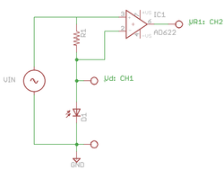
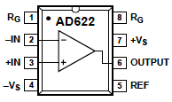
In this part of the lab, you will examine the examine how the I-V characteristic of a photodiode changes as a function of the amount of light falling on it. You will use a function generator and an instrumentation amplifier to make a simultaneous measurement of voltage across and current through the photodiode and plot both quantities simultaneously on an oscilloscope. The instrumentation amplifier is an integrated circuit that produces an output equal to the difference between the voltages at the two input terminals. The input terminals to the instrumentation amplifier have very high input impedance. Current flowing into the instrumentation amplifier inputs is negligible.
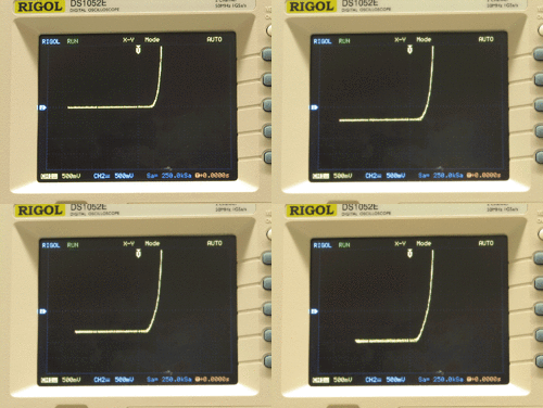
As shown in the schematic diagram, function generator V1 drives photodiode D1 through resistor R1. Since current flow into the instrumentation amplifier is negligible, current through the diode is equal to V1-VD1/R1. The output of the amplifier is equal to V1-VD1, which is equal to R1ID1. The I/V plot is obtained Using the oscilloscope's X/Y mode, with the instrumentation amplifier output (proportional to current) on the horizontal axis and the voltage across the photodiode V1{/sub> on the vertical axis.
Procedure
- Construct the circuit shown in the schematic above on a breadboard.
- Connect the power supply to power the instrumentation amplifier. Set the voltage to 15V.
- Connect the function generator to provide Vin to the circuit. Configure the function generator to apply a triangle wave between ± 1-3 V at 1 kHz.
- Connect the oscilloscope test leads to Vd on CH1 and VR1 (the output of the instrumentation amplifier) on CH2.
- Set the oscilloscope to X-Y display mode.
- In X-Y mode, the oscilloscope plots the voltage on the channel 1 input on the horizontal axis versus channel 2 on the vertical axis.
- With the photodiode covered, Capture the curve to a USB memory stick, load into Matlab and plot the real IV curve by converting the resistor voltage to current.
- Repeat the measurement for several intensities of light illuminating the diode.
- Plot the curves for all light intensities on the same set of axes.'
- What operating condition of the photodiode is best for measure light intensity?
</div>

